


Taiwan chip manufacturer TSMC to build third semiconductor fab in Arizona

09 April 2024
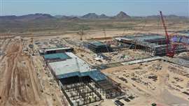 Progress on construction at TSMC’s fab in Arizona (Image: TSMC)
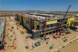
Taiwanese chip manufacturer TSMC has revealed plans to build a third semiconductor fab in Phoenix, Arizona, bringing its total expenditure on its factories there to more than US$65 billion.
The news came as TSMC Arizona and the US Department of Commerce signed a non-binding preliminary memorandum of terms for up to $6.6 billion in direct funding from the US government under the CHIPS and Science Act. The deal also provides up to $5bn in loans to TSMC.
TSMC Arizona’s first fab is set to begin production of chips using a 4 nanometre (nm) fabrication process in the first half of 2025. The second fab will produce chips using 2nm process technology with next-generation nanosheet transistors, with production starting in 2028.
The third fab will produce chips using 2nm or more advance processes, with production set to start by the end of the decade. Each of the three fabs will have a cleanroom area of approximately double the size of an industry-standard logic fab.
Increased investment in the three fabs is expected to create more than 20,000 accumulated construction jobs and tens of thousands of indirect supplier and consumer jobs.
Jensen Huang, founder and CEO of NVIDIA said, “TSMC has been a long-standing partner of NVIDIA since we invented the GPU and accelerated computing, and our ongoing innovation in Artificial Intelligence (AI) would not have been possible without them. We are excited to continue our partnership with TSMC as it brings cutting-edge facilities to Arizona.”

STAY CONNECTED


Receive the information you need when you need it through our world-leading magazines, newsletters and daily briefings.
CONNECT WITH THE TEAM